Join us back in San Jose in 2027!
21 - 25 February 2027
San Jose, California, US

Join us for another great event in San Jose in February

Participate in this annual symposium where leading researchers are solving challenges in optical and EUV lithography, patterning technologies, metrology, and process integration for semiconductor manufacturing and adjacent applications. Hear new research, challenges, and breakthroughs with your community once again in 2027.

The call for papers opens in June.

#SPIElitho LinkedIn icon Bluesky icon Instagram icon Facebook icon YouTube icon


Visa and invitation letter information

Make your event attendance smoother by submitting your paperwork early.
Get the details now.
Browse call for papers View highlights from 2026 event View highlights from 2026 event ...
Download call for papers Download 2026 program Download 2026 program ...

Explore six great conferences

  • Optical and EUV Nanolithography
  • DTCO and Computational Patterning
  • Metrology, Inspection, and Process Control
  • Novel Patterning Technologies
  • Advances in Patterning Materials and Processes
  • Advanced Etch Technology and Process Integration for Nanopatterning

Exhibition at Advanced Lithography + Patterning


Connect with the semiconductor community

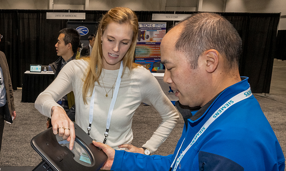
The exhibition at Advanced Lithography + Patterning is where people gather to collaborate and get business done. Find these technology solutions and more:
• Photoresist, EUV, and other specialty materials
• E-beam lithography systems
• Precision cleaning, contamination, transport support materials
• Wafer treatments and substrates

Student opportunities at the semiconductor conference


Students: learn how to attend this event for free

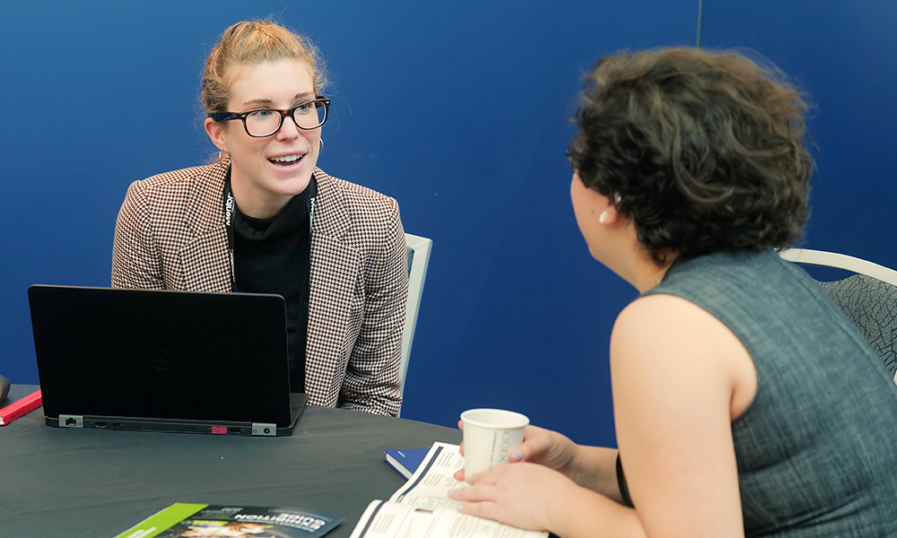
SPIE Advanced Lithography + Patterning offers numerous opportunities for students to engage with and learn about the semiconductor industry, as well as share their latest research in lithography and photomask technologies. Leading companies support student participation through grants and awards, and tech groups offer scholarships for graduate and undergraduate applicants.

Stay involved


Mail icon: Sign up for emails to stay informed about SPIE Advanced Lithography + Patterning Sign up for emails Sign up for emails ...
Phone icon: Find the SPIE app that keeps you connected to Advanced Lithography + Patterning Get the conference app Get the conference app ...