For science fiction to become science fact, particularly as envisioned by such authors as Philip K. Dick of the classic, Do Androids Dream of Electric Sheep? we are going to rely on substantial advancements in artificial intelligence (AI). However, even as we progress further into the newly proclaimed Age of AI and prognosticate vigorously on the possible outcomes, ranging from an idyllic utopian existence to the extinction of mankind, there is one generally agreed nearer term issue on which sentient beings of both human or replicant origin appear to be well aligned.
All AI-related systems appear to have an insatiable appetite for power. Their ever-increasing processing operations or calculations generate sufficient waste heat to inhibit the systems’ processing power. For starters, AI growth appears gated by approaches to address inefficiencies in operational design, architecture, and hardware to resolve overwhelming power and heat factors of current device performance scaling.
With Moore’s law on borrowed time and new viewpoints, such as Dennard scaling, forcing questions about current technology paths, it is inevitable that we hear renewed calls for the demise of the Silicon Age. But who shall this mantle of material age be passed onto? One upstart contender is that of 2D materials. Although best known for its champion, graphene, 2D materials are now technically considered as a whole class of inorganic compounds with the ability to exist in one-atom-thick layers called MXenes (pronounced Max-eens). This class of nanomaterials provides a smorgasbord of bandgap engineering enabled at the single-atom level.
All exciting, but does this mean that AI can be the killer-app that ushers in the 2D Material Age? Maybe. However, it is now clear from industrial level activities that bets are being placed that these materials are not going to be bystanders should silicon choose to give up its title.
Let’s just remind ourselves of the fundamental problem facing AI processing right now. Processors are generally based on Von Neumann architecture where processing instructions and parameters are iteratively fed from memory structures into a CPU to perform calculations. Traditional CPUs can consume more than 90% of their power solely in transfer of bits to and from the memory. Temperature sensitivity precludes memory being placed close to this core leading to CPUs being limited by memory latency and bit transport rather than processing speed—the Von Neumann bottleneck or memory wall.
Solutions to this interconnect problem are many. Notably, recent announcements would suggest an acceleration of near-term focus on silicon photonics and indium phosphide (InP). NVIDIA, the AI behemoth, recently announced collaborations with predominant players in the optoelectronics space, Coherent and Lumentum, to develop volume manufacture of photonic integrated circuits (PICs) based on silicon CMOS processing integrated with InP, active laser, photodetector, and related components. Utilizing photons rather than electrons in data transmission effectively removes the Von Neumann bottleneck or memory wall and hands AI performance control back to the processor. Chalk another potential win to materials science. However, with the Jevons paradox in play, wherein efficiency improvements simply lead to even higher consumption, it looks like we may need new materials to address faster processing solutions. Cue graphene et al.
Graphene, first isolated in 2004, has been proposed for myriad electronic and optoelectronic devices. Physics is on its side. The single layer of hexagonally arranged carbon atoms is strongly bonded in-plane leaving weakly bonded carrier electrons loosely bound both above and below. The unique symmetry and energetics of this arrangement impart a long laundry list of superlatives that can be applied to this zero-bandgap conductor. In its pure form, it is the strongest, stiffest, and most conductive material known. We can add infrared to ultraviolet broadband high-speed optics based on electro-absorption or plasmonic waveguiding. Finally, despite officially being a semi-metal, it also displays transistor-like behavior but with nuances to allow consideration into neuromorphic computing and nonvolatile memories.
Yes, it can in theory do it all. So, given this gift of a material from mother nature, why are graphene companies not common household names? Well, unlike applications that exploit the mechanical properties of graphene as an additive in a host matrix, such as concrete, electronic and optoelectronic applications with carrier mobilities more than 100 times that of silicon require atomically pristine films. Wafer-scale manufacturing further demands that this quality extend over commercially sized substrates ranging from 150 to 300 mm in diameter. Establishing these basics has been a journey, but now seems to have reached key milestones needed to spawn a new paradigm in graphene-based manufacturing. Rather than relying on industry-shared processing vehicles such as the European 2D pilot line, more companies, at great expense, are backing their own success by building dedicated, IP‑retentive manufacturing facilities.
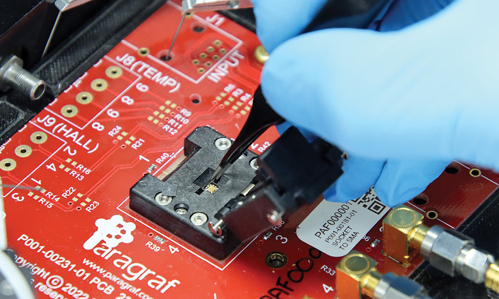
Paragraf, already a commercial graphene sensor manufacturer, has recently announced initial output from a purpose-built facility within the Cambridge, UK-area semiconductor cluster. Similar to other graphene electronics enterprises, but utilizing proprietary metal-free graphene growth, Paragraf has demonstrated graphene films that enable a variety of commercial devices including Halls sensors that operate in quantum computing environments and graphene field effect transistors that enable rapid and highly sensitive molecular detection across a universe of applications. This new 150 mm facility aims to provide significantly expanded access to these pristine films through a foundry-based capability for electronic- and opto-electronic based users alike.
Somewhat more impressively, Black Semiconductor appears to be rolling out two dedicated 2D material fabs in Germany. Nearer term is a 200 mm fab in Aachen, to be followed by a 300 mm fab in Dresden within the next two years. With the express intent to provide electronic PICs based on 2D materials for AI integration, Black Semiconductor appears to be the most visible of the standalone 2D dedicated entities forging the AI future. Other, more-established players such as TSMC, Intel, and Samsung, however, are forging ahead in the background. It is this new commitment to standalone 2D material manufacturing scale-up that augurs well for this new age.
We are still far from the visions projected by sleepy androids portrayed on-screen in the film Blade Runner. AI has a long way to go. Materials will continue to play a major role and 2D companies are stepping up to this challenge. It would be nice to think that those C-beams glittering in the dark by the Tannhauser Gate noted by Roy Batty on his last rainy day, may refer to the six membered rings of graphene that made it all possible.
Time to stop.
Andy MacInnes is Chief Development Officer at Paragraf.