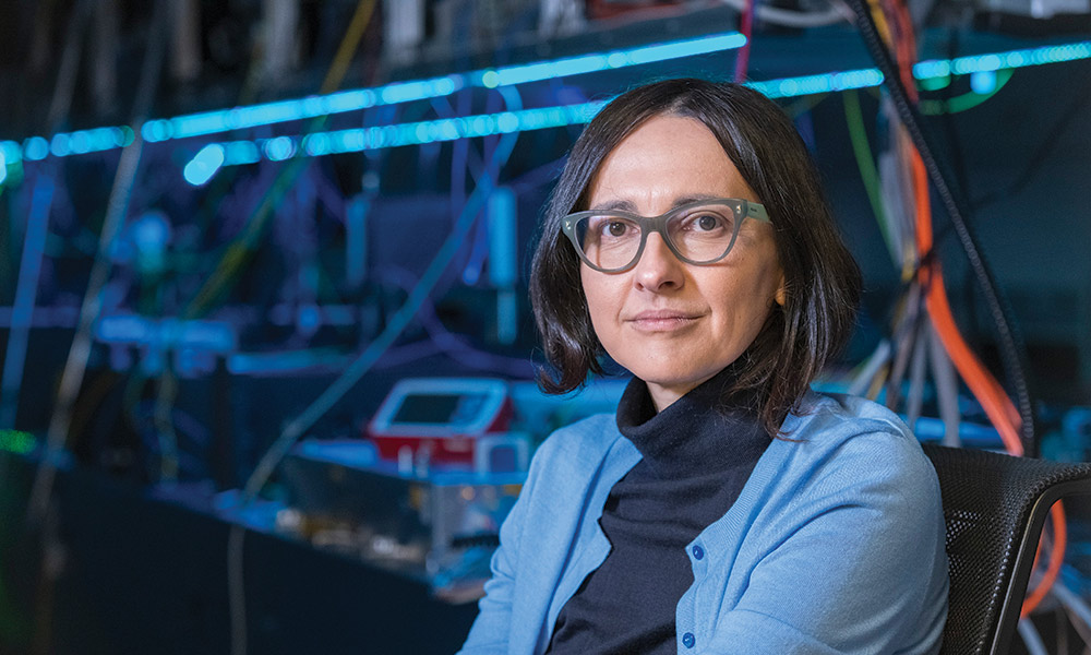
The concept of integrated photonics emerged in 1985 as a way to optimize the fiber-optic networks that were spreading around the globe. The benefits of integrating electronics were already evident, so integrating photonics with them seemed like a good idea. Yet it took decades before one of the field’s leading pioneers, Jelena Vučković, finally got the new technology off the ground. She did so by combining the bright ideas of applying classical information theory to optical devices and putting quantum optical devices on chips.
Integrated electronics and fiber-optic communications developed almost in phase in a series of successes through the 1970s and ’80s. After Richard A. Soref proposed silicon photonics, many assumed silicon and photonics would combine easily. An excellent example was the high transparency of silica at the 1.55-µm line of erbium-doped fiber lasers and amplifiers used for long-haul transmission. Intel and DARPA (Defense Advanced Research Projects Agency) were enthusiastic about the prospects for silicon-based light emitters for silicon photonics.
Yet the road was not easy. You can’t make silicon lasers because the electrons cannot move directly between energy levels without violating the conservation of momentum. Silicon can emit on Raman transmission, but it’s inefficient. You can make a silicon laser by making a diode laser from III-V semiconductors and bonding it to a silicon substrate, but bonding such materials is tricky.
Vučković didn’t have photonic integration in mind when she began her graduate studies at Caltech in 1996. A native of Serbia, her initial interest was in the applied math of information theory for the error-correction codes needed for high-speed fiber-optic transmission of data.
Vučković’s interest changed after she met Axel Scherer at her qualifying exam for the PhD program. A co-inventor of the VCSEL while at Bell Labs, he had joined the Caltech faculty, where he was one of a handful of people making photonic crystals to investigate them as resonators and build nodes for quantum networks. The concepts of their links to condensed matter physics and their manipulating light intrigued Vučković, and Scherer became her doctoral advisor.
Vučković was in the right place at the right time because her interests and prior training eased her into Caltech’s cutting-edge program. She had strong backgrounds in electromagnetism and physics, which helped her master photonics. Photonic crystals were just emerging on the nanophotonic research frontier, with only John D. Joannopoulos at MIT and Eli Yablonovich, then at UCLA, leading other groups. She recalls being “really intrigued by the connection between photonic crystals and condensed matter physics, where you could manipulate the flow of light.”
With Scherer and two other Caltech professors, quantum optics pioneer Jeff Kimble and quantum information theorist John Preskill, Vučković worked to build quantum networks, which transmit quantum information in the form of qubits, between quantum devices. “It was really applied quantum mechanics. That brought me deeper into quantum optics, and I started thinking about artificial atoms and solid-state systems,” to see what could be done with them,” says Vučković.
After graduation, Vučković’s interest in error-correcting codes and quantum optics and networks led her, in 2003, to Stanford University, where “everything kind of clicked,” she says. She joined the faculty of the university’s electrical engineering department where she formed research groups on both integrated photonics and quantum optics.
Today, Vučković is the department’s Jensen Haung Professor, head of its Nanoscale and Quantum Photonics Lab, and founder of Stanford Photonic Inverse Design Software, a spinoff based on a design technique which optimizes performance of photonic devices now being used in industry.
Says Vučković, “I develop quantum systems on a chip, equivalent to atomic physics systems but by using naturally trapped artificial atoms (impurities) in semiconductors.”
In July 2025, Zeiss recognized Vučković and Yuri Kivshar of Australian National University with the 2025 Zeiss Research Award for “outstanding work in the fields of nano- and quantum photonics.”
Vučković joined the Stanford faculty at a time when installation of fiber-optic communication cable slowed dramatically but internet traffic was soaring and communications carriers were demanding more bandwidth, higher data rates, and more information processing capacity. That required advances in both electronics and photonics. Photonics offered high-volume transmission of optical signals at light speed, high frequency, and low transmission loss. Integrated electronics processed and transmitted signals at high data rates. The question was how to combine electrons and photons to process signals and deliver them around the globe.
“The main school of thought was that everything you needed for optical interconnections could be done in silicon and materials compatible with CMOS silicon systems,” says Vučković. The buzzword was silicon photonics, and their focus was on the silicon. Although silicon was known to be a poor light emitter, the silicon industry was gigantic compared to the photonics industry and the expectation was that its technology could overcome silicon’s limits to dominate interconnection of fiber-optic network elements.
Vučković thought otherwise. After two decades of development, silicon-based materials still retained troublingly high light loss, limiting their optical ranges. She experimented with new materials and different ways of connecting photonics with silicon. “Bringing in new materials brings in new functionalities,” she says. In 2007, her group developed a photonic crystal laser based on III-V semiconductors. The laser was a two-dimensional nanostructure based on quantum physics designed to show that it could generate light more efficiently than silicon-based devices.
The success of the photonic crystal laser experiment demonstrated a crucial principle, Vučković says. “Photons are the best carriers of information, and you need them in order to network quantum systems. So, we need photonics everywhere, even if we are just working at [low energy] microwave frequencies or with atoms.” Using III-V semiconductors improved emission efficiency and performance. Adding new materials can add new optical and electronic properties and creating such heterogenous properties can be important in classical photonics as well as quantum systems.
The first integrated photonics to become available in the late 2000s had less than 50 active elements. Since then, the number of active elements have climbed at a rate paralleling Moore’s law growth. Like their electronic counterparts, integrated photonics are finding applications beyond their originally intended destination.
The materials being used now in integrated photonics are largely ones well known from their earlier uses in electronics and photonics. They include silicon on insulator (SoI), silicon nitride (SiN), indium phosphide (InP), silicon carbide (SiC), and silica (SiO2). Optical loss has been reduced but still remains a concern. Loss per-unit-cell now is 0.3 to 0.5 dB per thousand-unit cells, and some emerging applications will need that loss to be reduced to below 0.15 dB.
Many different materials are being investigated for future integrated photonics. Vučković’s group has demonstrated lasers on a chip based on titanium-sapphire and thulium-doped compounds. They also demonstrated erbium-doped oxide lasers and amplifiers integrated on top of silicon. New components that might be built into future integrated photonics are in the mill. In October 2025, her group reported in Science that strontium titanate cooled to cryogenic temperatures can have an electro-optic effect 40x stronger than that of lithium niobate. Vučković speculates that such materials could be used in arrays of optical tweezers for superconducting quantum systems.
Many more prospects building on Vučković’s achievements may await in the future, including integrated photonic tools for measurement and monitoring, reductions in power consumption by vast AI data centers, and new developments in basic science.
Jeff Hecht is an SPIE Member and freelancer who writes about science and technology.