While standard patterning approaches continue to prevail, the 2026 SPIE Advanced Lithography + Patterning conference, which ran 22-26 February in San Jose, California, also covered novel patterning technologies. Two presentations, in particular, illustrated the power of these emerging methods.
On Monday, Douglas Resnick, vice president of marketing and business development at Canon Nanotechnologies, started his keynote presentation, “A novel approach for the planarization of advanced semiconductor devices,” with the question, “Why does topography matter?”
To the unaided eye, a chip looks flat. But when the view zooms in to the nanoscale, patterned semiconductors are full of hills and valleys, some of which may be deep. Together these two contributors lead to height variations that can run in the tens of nanometers.
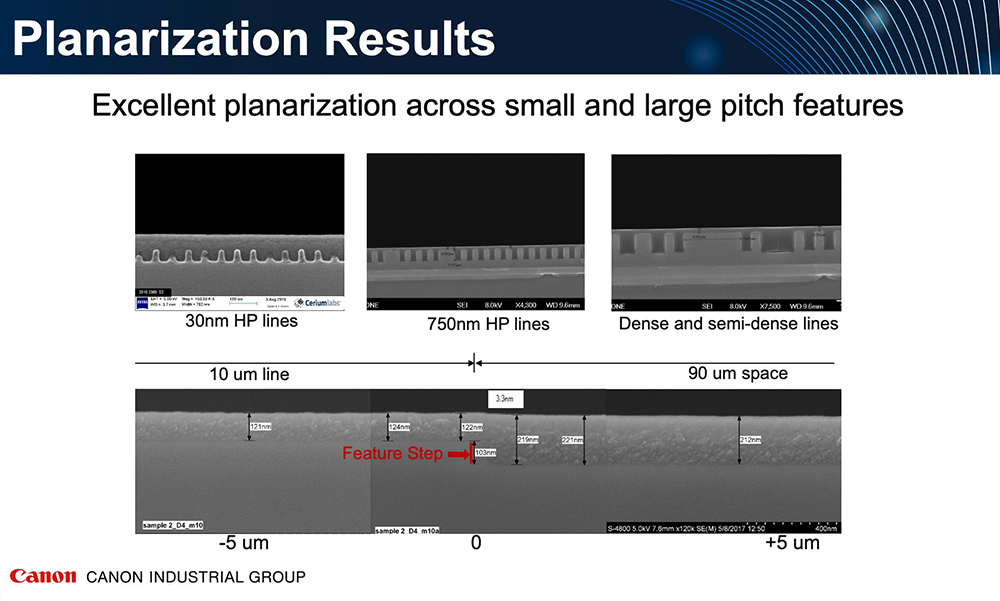
This topography impacts chip yield and performance because the tools printing patterns on the chip have a limited depth of focus. The semiconductor industry uses an abrasive process to polish out these height differences where possible. However, such corrective measures cannot happen at all steps in the manufacturing process. Another technique employed is to spin a dissolved carbon onto the chip, and this spin-on carbon flows over features and covers them with a film, creating a flatter surface . But this approach works best with small dense features; it has trouble with large features or areas where pattern density abruptly changes, according to Resnick.
In his presentation, he discussed a new approach developed by Canon Nanotechnologies that builds upon the company’s nanoimprint lithography technology. The new planarization method begins with an inkjet squirting small drops across a wafer, with the number of drops adjusted as the nozzle moves to bring each area up to the same height. A glass wafer is then placed in contact with the fill material. After that, the fill is cured so that it becomes rigid, and the glass wafer removed.
In testing done with a prototype tool, the technique improved planarization, dropping the height deviation from 12 nm or more to about 2 nm. Canon Nanotechnologies is now working on a tool for high volume manufacturing that will be available next year.
“This is a very enabling technology,” Resnick said. He noted that the technique can be used where having a flatter surface will help.
In a presentation on Wednesday during the conference, Clifford Engel, a technology research engineer at Intel Corporation, discussed maskless lithography and its application in semiconductor manufacturing. The lithography that mass produces chips involves a mask used to pattern photoresist on a wafer. Follow-on processing transfers the pattern to underlying films. Repeating these steps over and over creates a functioning chip.

In the maskless approach, a beam of either electrons or photons moves across a wafer and directly writes the pattern into photoresist, with the rest of process being the same as used in the masked approach. Without the cost and delay of producing a mask, trying out a new pattern is fast and adjustments to the pattern are easy to do.
According to Engel, a maskless approach can allow rapid product iterations because there is no need to wait for mask set construction. What’s more, the expense for small runs is low, creating situations where maskless is cost effective.
“If a low number of wafers are needed, maskless makes more sense,” Engel said.
In his talk, he outlined cases where Intel has used maskless lithography as a complementary technology that supports the masked approach used for high volume manufacturing. For example, the ability to print lines and spaces varies across a wafer. Hence, it is hard to tell just how far a process can be pushed and still have acceptable device yield. To solve this issue, a maskless tool can produce an array of lines and spaces, with these written at specific sites on a wafer. This array and its locations can be changed as desired, making it easier to do structure studies during process development.
Another example discussed by Engel considers the question: How can a technologist be sure that a measurement tool detects a defect? Perhaps there are no defects and so nothing shows up, a possibility in a high yielding line. But perhaps there are defects and the measurement tool misses them, a situation that brings risks of shipping faulty products.
With the maskless approach, a defect can be written on the fly into the photoresist. An example might be an electrical contact that is deliberately missing, with the location adjusted as needed. Knowing where the defect should be enables an evaluation of the testing method.
This capability is important and solves a problem, Engel noted. “Proving a negative is a huge challenge in the metrology space.”