Chip makers use lithography throughout the manufacturing process, which means lithography improvements are crucial to the semiconductor industry’s continued success. Two presentations at the 2026 SPIE Advanced Lithography + Patterning conference in San Jose, California illustrated some of the diverse efforts to create better lithography.
In a morning keynote, “Beyond scaling: High-NA EUV, EPE and stochastic control for the age of AI," Senior Manager of Patterning and Bonding Solutions at IBM Semiconductors and SPIE Senior, Luciana Meli, discussed how and where high numerical aperture extreme ultraviolet (NA EUV) lithography can benefit chip makers. While not a commercial chip company, IBM Semiconductors nonetheless is interested in furthering the manufacturing of state-of-the-art semiconductors. Such devices are used in IBM’s high performance, high reliability computing products.
“Our mission is to create what is next in computing,” Meli said during her talk.
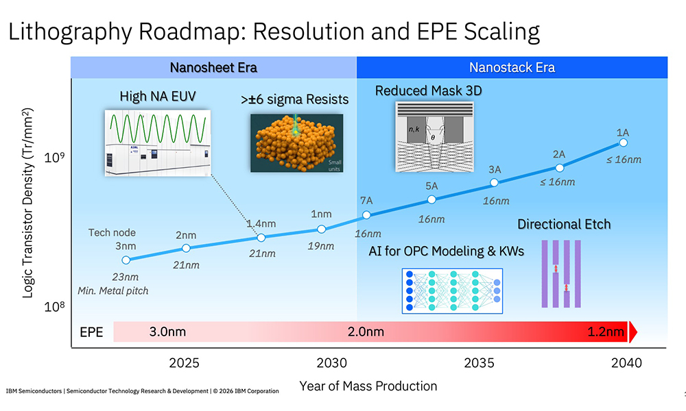
High NA EUV is the latest version of the 13.5 nm wavelength extreme ultraviolet lithography that is used to pattern the most demanding chips layers. It’s called high NA because the process has a numerical aperture of 0.55, as compared to the 0.33 NA of the first commercial version of EUV. The higher the numerical aperture, the smaller the features a lithography tool can print. A 0.55 NA system, for example, can print 40 percent smaller features than a 0.33 system.
In discussing high NA EUV lithography, Meili said that what is now constraining chip manufacturing is not the ability to print ever smaller features, but instead it is how well each layer aligns to the ones below it, with this measured by the edge placement error. Minimizing this number requires process control, and high NA EUV is fundamental to that because it helps improve process control, according to Meli.
The higher resolution of high NA EUV also makes it possible to print the most exacting circuit layers in one pass, as opposed to doing a double pass where each pass prints half the pattern. The double pass tactic has been used when absolutely necessary because of lithography limitations. However, it is slow, costly, and leads to a wider spread in chip performance. The industry was considering double pass low NA EUV, but the arrival of high NA EUV changes the calculation, even though the new lithographic tools are larger, more costly, and cost more to operate than those of the previous technology.
“The advantage of high NA is obvious. You get much higher yield,” Meli said in summing up the effect of the new lithography systems.
Getting the latest patterning technology entails more than just lithography tools that are bigger than a double-decker bus. The right molecules are also needed, with an example being those found in the photoresist. When exposed to light of the right wavelength, photoresist materials change composition. Follow-on processing transfers that photoresist pattern into the film of a wafer, creating a layer of what will eventually be a chip.
With high NA EUV now here, suppliers are rolling out suitable photoresists. In his afternoon presentation, Alexander Marwitz, senior staff chemist at Inpria, discussed the company’s metal-oxide photoresists in his talk, “Metal-oxide resist material and process advancements for positive- and negative-tone high NA EUV lithography applications”.
He noted that light striking the molecules breaks some of the bonds, which changes the material’s characteristics. Mixing in additives can make the photoresist more sensitive, enabling a lithography tool to expose a pattern using a lower dose and thus saving money. Additives can also help reduce line edge roughness, helping minimize lithography limiting edge placement error.
Inpria’s photoresist is versatile, Marwitz noted. “Our material and platform are capable of being negative tone or positive tone.”

A visualization of formulation and process co‑optimization showing how ligands, additives, and process conditions interact to enable MOR material performance.
In a positive tone resist, areas exposed to light develop away. Thus, what ends up on a wafer matches what is on the mask. Using a negative tone resist leads to opposite effect. What is on the wafer is a negative of what is on the mask.
Inpria is currently optimizing its positive tone resist, changing additives and making other adjustments to improve the resist, according to Marwitz. He said a key reason to doing so is to improve local critical dimension uniformity. A critical dimension is a feature size, such as the width of a contact hole, that determines if and how well a circuit functions. Keeping such dimensions more uniform improves yield.