Whether you are excited or terrified by the AI revolution, one thing is certain: It is here. Most prominently, generative AI tools like Open AI’s ChatGPT, Google’s Gemini, Microsoft’s Copilot, and the rest are infiltrating more and more aspects of modern life. But this permeation presents a practical problem. At its current rate of growth, AI’s computing demands are simply not sustainable.
The extent of this problem cannot be overstated. According to a McKinsey report, global data center capacity from AI workloads will increase 3.5 times by 2030 to 156 GW, more than the entire current energy demand of France. Delivering the data center infrastructure to meet this capacity increase will come at an eye-watering cost, too: $5.2 trillion between now and 2030.
“It is challenging to support the increasing demand from this kind of computing power, but more important is the energy consumption,” explains Tsinghua University computational optics expert Lu Fang. To illustrate the problem, Fang uses the example of OpenAI training its GPT-4 system. “The energy consumption was around 13 million kilowatt hours of electricity, which is the equivalent of 4,550 tons of coal.”
“There are data centers that are being built for AI training that use as much power as the biggest cities on the planet,” says Nick Harris, CEO of Lightmatter. “If you look at Earth from space, some of the brightest objects [in the thermal infrared] you’ll see are data centers—the only things brighter are volcanoes and deserts.”
Humanity could, of course, take a pause or attempt to moderate AI usage. But this is very much not in our nature. “Researchers working on algorithms, neural networks, and deep learning will not stop,” says Fang. “In fact, they are continuously scaling up model depth and parameters, pushing toward artificial general intelligence,” or AGI, a type of AI that could theoretically learn any intellectually demanding task at or beyond the level of human capability.
So, with the march of technology showing no sign of slowing, if anything accelerating, how can society keep up with AI demands while addressing the huge economic and environmental burden this will inevitably bring? One way is to break the problem down to its core. Fundamentally, the culprit limiting computing power is the mainstay of information processing—the venerable electron. It is the bottleneck limiting the speed and memory bandwidth needed to perform calculations and process information and causing this staggering energy consumption. Is there an alternative?
The answer is yes, with caveats. Photons are massless and therefore travel at the universe’s speed limit, light speed. Being fundamentally faster than electrons should mean photonic computers in theory could speed up operations by six to eight orders of magnitude compared to electronic computers. Moreover, photonic systems have the potential to offer more bandwidth and run more computing steps in less time and with less latency than their electronic counterparts.
These advantages have the potential to vastly improve computing efficiency. Light doesn’t need to pass through any materials to get from A to B, unlike electrons that collide with ions along their way, generating heat. Despite requiring lasers, which generate waste heat, to function, photonics systems have the potential to be much more efficient and generate much less heat than their electronic counterparts.
Of course, you would be reading this article on your photonic computer right now were it not for a “but.” Photonic computing has been an active topic of research for more than half a century, but only now are the first practical products entering the market. The reason is that replacing electrons with photons is not like switching your old incandescent light bulbs to LED bulbs. As Photonics Focus readers will be acutely aware, photons have fundamentally different characteristics than electrons. For example, photons generally don’t interact with each other, making what you would think of as even the simplest job, like engineering a photonic transistor, immensely challenging.
The most basic application of a transistor is using it as a switch. But switching in a photonics system currently requires one light beam to control another, and this can only be done through nonlinear optical effects. Typically, however, nonlinear effects either manifest at light intensities too high for photonic computing, or they require the use of specific strongly nonlinear materials not well-suited or developed enough for large-scale production. As a result, researchers are still searching for materials and mechanisms that could achieve efficient and practical photonic switching.

An integrated photonic chip system. Photo credit: Tsinghua University.
While photonic transistors can’t currently achieve nonlinear switching, photonics systems are good at matrix multiplication, which underlies neural networks. This is the primary reason why some of the first breakthroughs in neural networks were made with photonics systems. Around the time CERN was launching the World Wide Web in 1993, a team at the California Institute of Technology was building an optical network capable of recognizing the identity of faces. The two-layer optical network took images of faces as input at standard video rates and classified them. Trained by gradually adapting photorefractive holograms based on video recordings of one of the researchers, the network could discern recordings of this researcher from other members of the team in real time with remarkable success.
Though followed up by incremental improvements, interest in optical neural networks started to wane at the end of the millennium, as digital computers left analog photonics systems in the dust. Recently, though, researchers have been reevaluating photonics systems as vehicles for processing large amounts of information in parallel and at high data rates in real time.
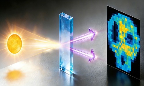
Aydogan Ozcan of the University of California, Los Angeles, has been at the forefront of these efforts for the best part of a decade. In 2018, he and colleagues published a seminal result in Science. “That was the first demonstration of optical processing through structured materials for computing, for statistical inference, for classification of different types of objects,” he says.
Ozcan explains that his neural network was formed by multiple layers of diffractive surfaces working in conjunction to optically perform an arbitrary function that the network could statistically learn. The network was created using several transmissive and/or reflective layers, where each point on a given layer either transmitted or reflected the incoming wave. Trained via computer simulation, the layers were iteratively adjusted towards performing a specific machine-learning task until all of the transmission or reflection coefficients were determined, so that collectively the network would be able to perform that task solely through light-matter interaction and optical diffraction. At this point, all the parameters were fixed, and the physical network could be built, either using 3D printing or lithography.
Though the network’s training was done digitally, inference, i.e. applying the trained machine learning model on new, unseen data to generate predictions or decisions, was all-optical. “This is a diffractive processor where the analog information comes in the form of photons, meaning the information that I want to act on, classify, recognize, compute, or form a computed image [of] in any way, is really carried by photons,” Ozcan explains. “At the output, I don’t want it to give an image to do standard classification with a digital network, I want to use a material that is fabricated at a wavelength scale to process the information content of that wave as it’s diffracted, so it can, say, send photons right if the image is of a human or left if not.”
As described in the 2018 paper, to demonstrate the power of all-optical inference, Ozcan’s team successfully trained and demonstrated diffractive processors capable of automatically classifying both handwritten digits from 0 to 9, as well as fashion products, all of it operating at the speed of light, using only passive optical components and diffraction.
Since then, Ozcan has taken the research to the next level, with a particular focus on machine-vision applications. He says that the current paradigm in machine vision—from analyzing tissue samples in biology, to checking for defects in pills on the pharmaceutical factory floor—is to capture and digitize everything about an object or sample of interest. The result is a data deluge across a host of industries. Diffractive processors solve this in one fell swoop, because they don’t capture data until an event happens.

Conceptual illustration of fully forward-mode photonic training. Photo credit: Tsinghua University.
“We started out with terahertz waves because they are spectroscopically very rich, and they can also see through visibly opaque materials like plastic and paper,” says Ozcan. “With a diffractive processor operating in the terahertz regime, without creating a 3D image or tomogram, we showed that you can see through opaque 3D objects and identify defects hidden in the volume which traditional infrared machine vision would miss.
“Think of the implications of this for pharmaceuticals—tremendous opportunities,” Ozcan continues. “If we have a drug, without opening the packaging or even capturing an image, we can answer, ‘Does it have a defect or not? Do we have the correct dose or not?’”
Though potentially transformative for machine vision, particularly when extended to other exciting applications utilizing wavelengths beyond the terahertz domain, Ozcan’s diffractive neural networks remain fairly rigid in terms of their ability to perform only specific, limited tasks. Other research groups are exploring new approaches to making optical neural networks more flexible and powerful in order to solve more complex tasks, with a view to perhaps even surpassing electronic systems and achieving the “holy grail” of building an optical neural network for AGI applications.
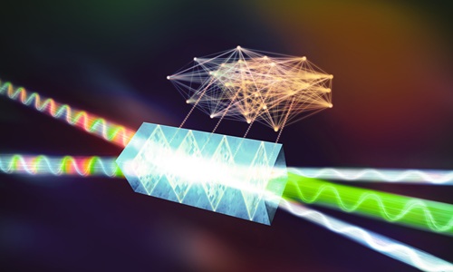
One group is led by Fang. A year ago in a Science paper, they introduced Taichi, a photonic chiplet specifically designed to complete AGI tasks. “When we were working on Taichi, we figured out that if we just mimic existing approaches and try to build up a very deep neural network, it cannot work,” she explains. “Photonic computing is analog computing, whereas conventional electronic computing is digital computing, where errors are automatically suppressed.”
The team realized that simply increasing the number of layers, as you would do for an electronic architecture to increase performance, only meant that errors increased. “That’s why previous photonic computing work could only solve very simple tasks,” Fang adds.
Like Ozcan’s optical neural networks, Fang’s Taichi takes advantage of diffraction, but also another property of photons: interference. “Diffraction can help us to achieve massive computing, and interference can help us to achieve reconfigurability,” says Fang. “Combining these allows us to use one chip for very large-scale computing applied to multiple different tasks.”
In the paper, Fang’s group described the experimental realization of Taichi, building an on-chip 13.96-million-neuron optical neural network. They then demonstrated Taichi’s capabilities. First was a demonstration of classification, but at much larger scale than earlier achievements: 1,000-category recognition. Next, they demonstrated higher functionality by guiding Taichi to generate content. “We showed that Taichi is able to solve the tasks of image or audio content generation,” Fang enthuses. “For example, after training on Bach’s compositions, Taichi generated new music that emulated Bach’s style.”
Although it is a fully functional computing system capable of independently executing intelligent tasks, the Taichi chiplet is not yet a finished product. To move toward commercialization, several challenges need to be addressed to make the system more robust and integrated, for instance, by incorporating on-chip light sources.
“In a commercial chip, the lasers need to be miniaturized and integrated, which is a task that requires collaboration with industrial partners,” says Fang. In addition, despite all the computing taking place optically, electronic devices are still needed for buffering, storage, and control, and these would need to be optimized specifically for photonic computing in a commercial product. For these reasons, Fang is cautious about when a descendant of Taichi might be commercially released. “If you want a mature GPU-level photonic solution, I believe there is still a long and challenging journey ahead.”
With huge investment and hiring happening, the likes of Lightmatter and its competitors could have a say in accelerating this timeline. To huge fanfare, Lightmatter earlier this year launched two wafer-scale programmable photonic interconnect products, Passage L200 and M1000. Harris calls the latter “our crown jewel of interconnect technology, 114 trillion bits-per-second in a single chip, the largest photonic chip in the world.”

Lightmatter has introduced its Envise photonic chip. Photo credit: Lightmatter.
Though not chips designed to complete AI tasks, the Passage product family indirectly solves some of the problems plaguing AI models. “Have you ever used Deep Research in ChatGPT and noticed it takes 12 minutes?” asks Harris, referring to a fairly new feature in ChatGPT that uses reasoning to synthesize large amounts of online information and complete multistep research tasks. “Passage ultimately links together a huge number of GPUs, let’s say 1,000 or more, to run those heavy workloads and get you an answer back in one second, so it solves the communication bottleneck.” At the same time, incorporating Passage into the vast data centers being built for AI training, by the likes of OpenAI and others, makes that AI training faster and more efficient.
While Passage has been entering production, Harris and his still-growing team have been working on the next phase: Developing a photonics system to perform high-precision AI calculations. Details of the company’s Envise photonic processor were published this year. Similar to Taichi, Envise integrates photonic cores with conventional electronic control and memory systems, programmed using standard AI frameworks like PyTorch and TensorFlow.
Envise is higher on the technological readiness ladder, however, with 50 billion transistors and 1 million photonic components spread across 6 photonically interconnected chips in a single package. “No one’s ever built a practical computer that wasn’t based on transistors that can do anything useful,” says Harris. “And we wanted to share that moment with the world.”
In their paper, the Lightmatter team showed how Envise can execute advanced AI models to near electronic precision, including BERT (bidirectional encoder representations from transformers), a machine-learning framework for natural language processing developed by Google, and the Atari deep reinforcement learning algorithm, which has achieved a level comparable to that of a professional human games tester across a set of 49 classic Atari games.
But Envise is more of a research platform than a wannabe product. “We’re not going to market with photonic computing right now,” says Harris. “We’re looking at what the future of computing will look like because, ultimately, human progress on almost every front relies on computers getting better, and transistors are no longer getting better.”
Might this future see all-optical photonic chips delivering AGI? Despite significant progress on this front in recent years, Harris, Fang, and Ozcan agree that future computation, at least in the near term, will still involve some electronics. “Developing a photonic chip that functions like a GPU or CPU isn’t realistic at this stage,” says Fang. “Photonic computing and electronic computing must remain close allies.”
Benjamin Skuse is a science and technology writer with a passion for physics and mathematics whose work has appeared in major popular science outlets.